← All projects

Power and sensing electronics for a dual-deployment rocket

The team's rocket targets a 10,000 ft apogee and needs two parachute deployments at the right moments. I designed the board that powers the flight computer, reads its sensors, logs data and fires the deployment charges.

Team
Texas Student Rocket Propulsion Lab, 15–20 members
When
Feb 2026 – present
My role
Electrical architecture, schematic, PCB, BOM

What the board has to do

  • Run a Teensy 4.0 flight computer and its sensors from a single battery for the whole flight.
  • Measure altitude and motion, so the flight software can detect apogee and the main-deploy altitude.
  • Log everything to a microSD card for analysis after recovery.
  • Fire two deployment charges, drogue and main, only when armed and only when commanded, and report beforehand whether each charge is actually connected.

That last point drove the design more than anything else. A deployment circuit that fires early is dangerous, and one that doesn't fire loses the rocket.

Architecture

Click a block to see what it does and why I chose it.

Copper lines carry power. Thin dashed lines are data buses.

I2C SPI fire / sense 2S Li-Po7.4 V nominal Buck converterLM2596 3.3 V LDOclean logic rail Teensy 4.0flight computer IMU + BMP388motion, pressure microSDflight log Arm switch+ status LED Deploy channelsMOSFET × 2 + continuity UART debugbench only

How I chose components

For the sensors I compared candidates side by side in a decision matrix weighted toward reliability and noise performance. The matrices went into the design documentation, so reviewers could see why a part was chosen and not just which one.

Alongside the schematic I produced the wiring diagrams, pin maps and BOM, plus a list of validation checkpoints (continuity and signal-path checks) for when the board is built.

PCB layout
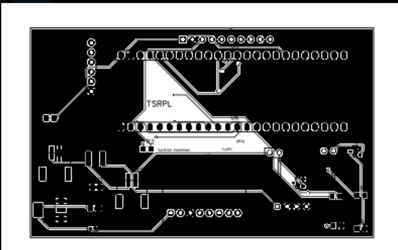
Copper layer of the avionics PCB: Teensy 4.0 footprint across the top, regulator and power components lower left, deployment channels lower right
Copper layer of the avionics board in EasyEDA. The two rows of pads across the middle are the Teensy 4.0 footprint, the power regulation sits in the lower left, and the deployment and connector circuitry is to the right. Designed and reviewed, not yet manufactured.

Status and next steps

Where it stands: the schematic, PCB layout and BOM are complete and were presented in design review. The board hasn't been fabricated, and sensor firmware and hardware bring-up haven't started. Nothing here has flown.

Next comes fabrication and assembly, then bring-up: verifying each power rail under load, checking every bus with a scope and logic analyzer, and testing the continuity and fire circuits with dummy loads long before any real charge is connected. I'll update this page as each step happens.

What I learned: on a team project, the documentation is part of the design. Clear pin maps and selection matrices let mechanical, software and electrical people make decisions without waiting on me.